Introduction
This document shows how to analyze HDMI (High-Definition Multimedia Interface) PCB layout design with PollEx SI (Signal Integrity) tool.
Background: HDMI Specification Version 1.3
HDMI system architecture
- The HDMI cable and connectors carry 4 differential pairs; 3 TMDS data and 1 clock channels (TMDS: Transition Minimized Differential Signaling).
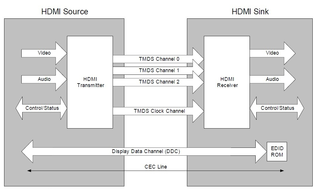
Fig. 1. HDMI Block Diagram.
Electric specifications
- One TMDS differential pair: Current driver at Transmitter (Tx), Pull up resistor at Receiver (Rx)

Fig. 2. Conceptual schematic for one TMDS differential pair.
Table 1. Required operation conditions for HDMI Interface.

- TMDS source requirements: Testing Point (TP1) on Board (PCB), Pattern = Layout design
Fig. 3. Balanced source test load.

Fig. 4. Eye diagram mask at TP1 for Source requirements.
Analysis: HDMI Layout Design with PollEx SI
- Explore HDMI Layout (Pattern)
- Tool > PCB Explorer > Net > CN-||MCU_HDMI_TX0P||SIGN.. ~ CN-||MCU_HDMI_TXCP||SIG...> Excl
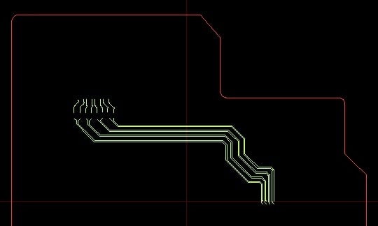
Fig. 5. HDMI TMDS Layout Design (Exclusive View).
2. Option > Net 2D/3D Viewer : Tx= U1 (IC-NXP4330), Rx= CN1 (47151-0001)
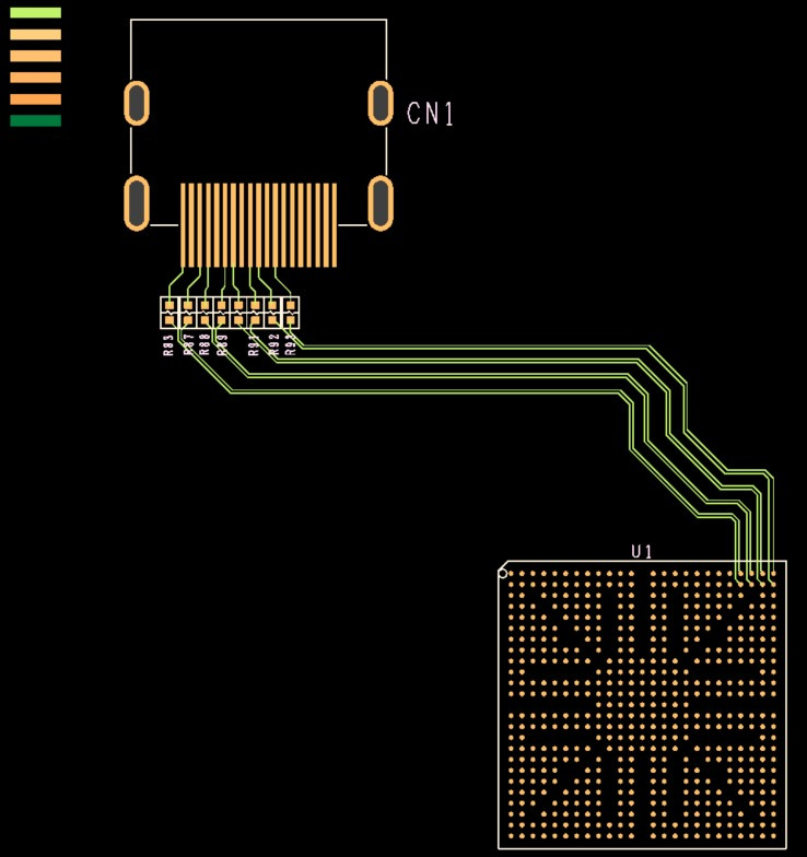
Fig. 6. HDMI TMDS Layout Design (Net 2D View).

Fig. 7. HDMI IBIS model for TDMS transmitter (NXP4330).
2. Properties > Parts > Double-click “47151-0001” > Device Model Files > Add “Connector_linear.dmf” > Click “Display” to open Linear Device Modeler > PU50_TO33
-
- Vcc = 3.3 V & Rin_p= 50 Ohm with reference to Fig. 2 and Table 1

(a) Model Spec

(b) Model Data
Fig. 8. Linear model for HDMI receiver (connector).

Fig. 9. Net topology for one HDMI TMDS layout
2. Analysis > Net Analysis:
- Active Driver Pin = U1_B24
- Pulse Period= 0.588 (nS) from the condition that “Max. bit rate for each TMDS data channel= 3.4 Gbit/S (1.7 GHz= Time period 0.588 nS)”
- Device Models: Input = PU50_TO33 & Output = hdmi_minimp_33_0000

(a) Overall setting

(b) Device Model setting
Fig. 10. Setting for Topology Network Analysis.
3. Check the final simulation results: Eye diagram
- Waveform: CN1_7 & CN1_9 - Vdiff
- Eye Mask setting with reference to Fig. 4: Height (V) = 0.5 (=0.25+0.25), Top/Bottom= 37 (=(0.68333-0.31666)*100), Middle width(%)= 70 (=(0.85-0.15)*100), Reference voltage = Ground

Fig. 11. Eye diagram (green) at HDMI connector with Eye mask (red).
References
Attachment: Solved PollEx SI Project.