In this example circuit, a phase-shifted full-bridge converter is implemented with a synchronous rectifier on the secondary. Peak current-mode control, PCMC, is implemented with a PI controller controlling the output voltage. This example is available in the example library of PSIM with this default path "Altair_PSIM_2025\examples\dc-dc" Other interesting features of the simulation are:
- Zero Voltage Switching of the primary side FET
- Zero Current switching of the secondary side FETs
- Soft Start ramp-up
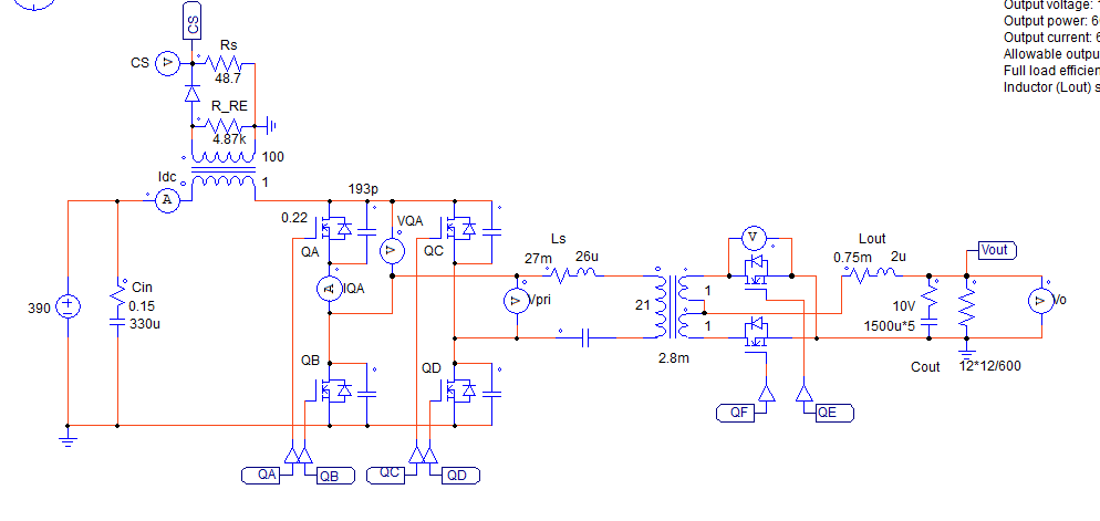
The design specifications of the power supply are:
Input voltage 390Vdc
- Output Voltage 12Vdc, 50A, 600W
- Allowable output voltage transient: 600mV
- Full load efficiency: 93%
- 100kHz FET switching
- 200kHz output inductor ripple
Soft-Start Implementation
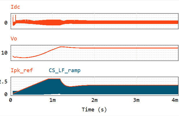
The soft-start is implemented with a current source charging a capacitor. The soft-start, soft_start_V, will start at 0V and rise while the output from the voltage controller, Vcontrol_output, will start at the op-amp rail voltage. With the orientation of the diodes, the soft-start voltage will dictate the peak current reference until the output from the voltage controller is of a lower magnitude. In the waveforms we can see peak current reference, Ipk_ref, start with the shape of soft_start_V before the voltage controller takes over. The ‘soft start’ reference voltage will need to be high enough so that it does not interfere with the normal operation of the supply, in this implementation, it will be 3.05V which is set by the addition of the reference voltage 2.5V and the voltage across the diode of 0.55V.
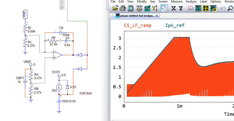
Peak Current Control Setup
A current transformer is used to monitor the input current along with a simple low pass filter and a diode to eliminate the negative portion of the current cycle and to provide leading-edge blanking to prevent the leading edge spike from causing problems with the peak current mode control.
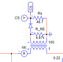
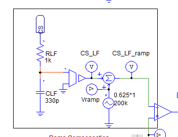
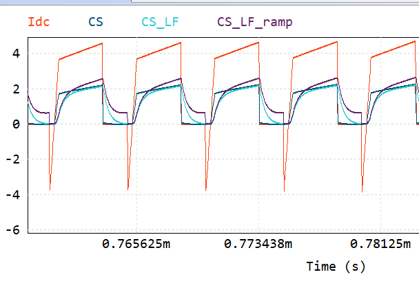
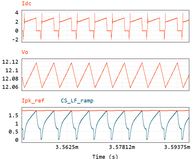
A ramp with a duty cycle of 100% and a slope of .125V /us or 0.625V peak per period has been added to prevent oscillations in the control loop with duty cycles above 50%. The waveforms are showing a few cycles of the input current Idc, the unfiltered positive side of the current sense CS, the filtered waveform CS_LF which is removing the leading edge spike, and the waveform CS_LF_ramp after the ramp has been added.
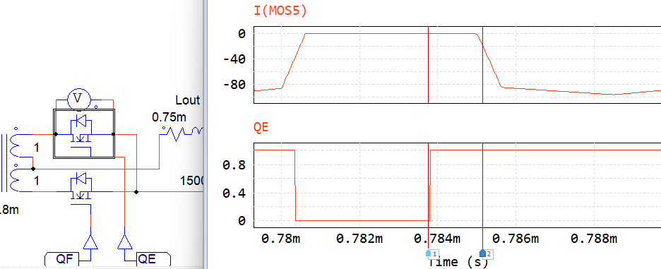
At standard operating conditions, the converter achieves Zero Voltage Switching, ZVS, on the primary high-side MOSFET and Zero Current Switching on the active secondary MOSFETS.
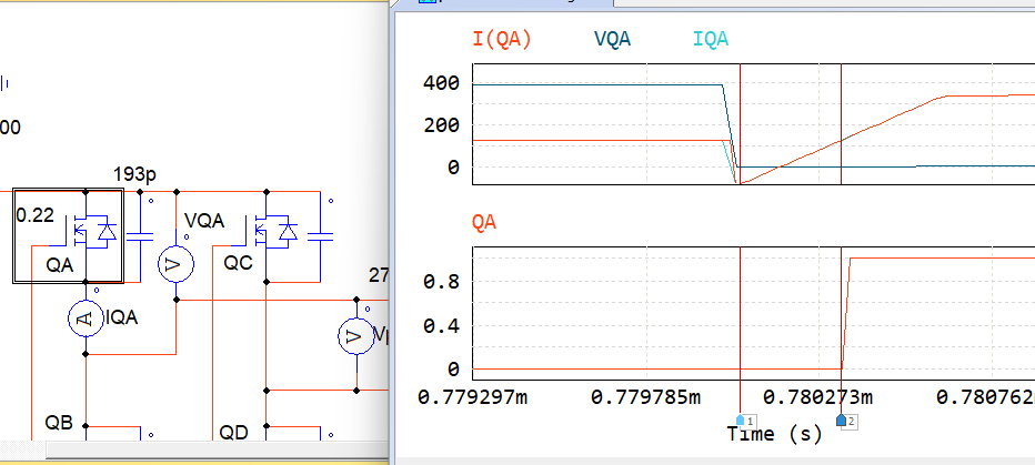
We are able to see that when the MOSFET QA is switched on the voltage across it is ‘0’ and the current starts to flow. This can be seen by comparing the rising edge of QA, the gating signal, with VQA the voltage across the switch.
We can observe the Zero Current Switching, ZCS, of the secondary by comparing the gating signal QE leading edge with the current flowing through the device I(MOS5), it can be observed the current is 0 Amps and does not start flowing until after the switch has been turned on.
Deadtime
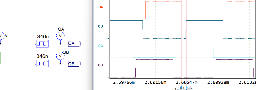
Deadtime of 346ns has been implemented in this circuit with a monostable multivibrator element, that has a pulse width of 346ns. This provides 346ns of deadtime to the leading edge of the gating signals. This deadtime is important as it allows soft-switching, ZVS, of the primary side top MOSFET to be achieved. The deadtime allows the inductor to force the node voltage to the rail causing the top MOSFET body diode to conduct, which then allows the MOSFET to be switched on with near-zero voltage across it.
Overall Operation
Here are the waveforms of the input current, output voltage, and the peak current reference from start-up to steady-state.
Below are the detailed waveforms at steady state, we can see that the ripple of the output voltage is constant and the peak current reference is stable.
Related Resources
Webinar on Phase shift full bridge code gen with HIL verification
AC sweep overview with PSIM