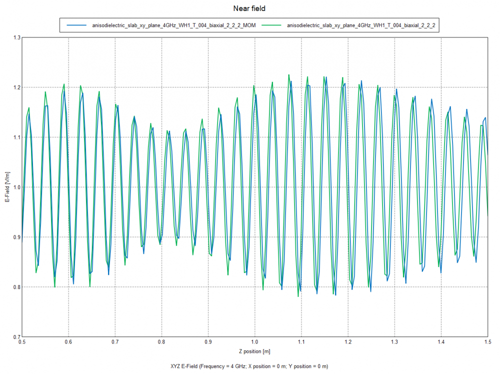
Anisotropic slab plane wave incidence shift in E field when using FDTD
Hi
I am modeling a thin bi-axial anisotropic slab with plane wave illumination using FDTD solver. In order to validate result from FDTD I made the anisotropic tensor to be isotropic and modeled the structure using MOM-MLFMM solver. When I compared the near field results I find a shift in total electric field for certain observation points. I have attached the model and postfeko file for your reference. Can you please have a look at the FDTD solver model and let me know if I have to change any simulation settings.
Thanks,
Shan25
Find more posts tagged with
Hi Mel,
Thanks for your reply. I tried modeling the structure using FEM solver. I get this error
ERROR 50058: Missing buffer zone for the anisotropic FEM region when coupling MoM and FEM
I don't have any MoM regions in the model. I get the same error message when enabling/disabling 'Decouple from MoM' in solver settings. Can you please explain the reason for this error message.
Hi Shan25
The FEM, for anisotropic materials, does not allow an anisotropic material on the FEM boundary. The workaround is you must enclose the material with a FEM air (epsr=1) isotropic dielectric.
Please view the two videos encircled below on https://altairuniversity.com/learning-library/
It will show how it is done.
<?xml version="1.0" encoding="UTF-8"?>


Hi Shan
I don't consider the shift to be unexpected. Perhaps you just need a finer mesh.
But then again you need to model the same in both methods. The FEM also supports anisotropic materials. You could compare FDTD with FEM.