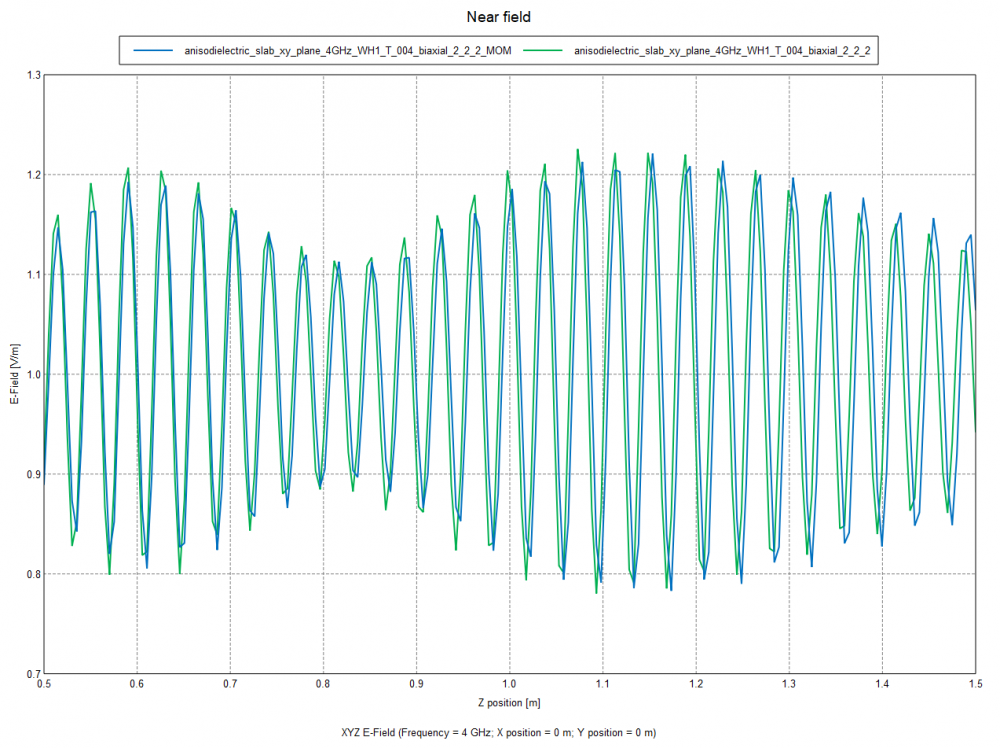
Anisotropic slab plane wave incidence shift in E field when using FDTD
Hi
I am modeling a thin bi-axial anisotropic slab with plane wave illumination using FDTD solver. In order to validate result from FDTD I made the anisotropic tensor to be isotropic and modeled the structure using MOM-MLFMM solver. When I compared the near field results I find a shift in total electric field for certain observation points. I have attached the model and postfeko file for your reference. Can you please have a look at the FDTD solver model and let me know if I have to change any simulation settings.
Thanks,
Shan25
Answers
-
Hi Shan
I don't consider the shift to be unexpected. Perhaps you just need a finer mesh.
But then again you need to model the same in both methods. The FEM also supports anisotropic materials. You could compare FDTD with FEM.
0 -
Hi Mel,
Thanks for your reply. I tried modeling the structure using FEM solver. I get this error
ERROR 50058: Missing buffer zone for the anisotropic FEM region when coupling MoM and FEM
I don't have any MoM regions in the model. I get the same error message when enabling/disabling 'Decouple from MoM' in solver settings. Can you please explain the reason for this error message.
0 -
Hi Shan25
The FEM, for anisotropic materials, does not allow an anisotropic material on the FEM boundary. The workaround is you must enclose the material with a FEM air (epsr=1) isotropic dielectric.
Please view the two videos encircled below on https://altairuniversity.com/learning-library/
It will show how it is done.
<?xml version="1.0" encoding="UTF-8"?>
0