Abstract
Altair Feko supports extensive cable modeling features, and this article will describe the latest features in more detail. The main cable feature is the combined MoM/MTL schematic link functionality. This allows accurate modelling of non-ideal (pigtail) shield connections to a device and radiation from common mode cable currents between connected devices.
Introduction
Cables between interconnected systems could be a significant source of EMC and modeling the connection of cables to structures (devices) are especially important as the frequency increases.
Modeling the fine detail of the cable harness wires, insulation and shields with a full 3D method could be computationally prohibitive. Modeling the cable with the Multiconductor Transmission Line (MTL) formulation [1] reduces the computational cost significantly. Effectively the cable is modeled with a distributed circuit and coupled to the 3D EM domain (solver). This is good approximation of the physics when the assumptions, of TEM propagation inside the cable itself and TEM propagation for the cable coupling to the surrounding environment, are valid. Feko will provide warnings when these assumptions are possibly violated.
Review of Feko cable modeling
The standard Multiconductor Transmission Line (MTL) formulation allows for efficient modeling of cable bundles above a conductive installation without the need of full wave modeling of the fine cable bundle details.
Cable modeling in Feko has significantly evolved since its introduction in 2006. It started with irradiation of cable bundles and steadily expanded to include radiation from cable bundles in 2008. The basic assumption of the MTL formulation is that the propagating fields inside the cable bundle and between the cable bundle and the installation is Transverse Electromagnetic (TEM). This limits the electrical height of the cable bundle above the conductive installation.
In 2010 the unique combined MoM/MTL formulation for shielded cable bundles was released and removed the electrical height restriction of standard MTL above the installation.
In 2012 the coupling between the MTL and full wave domains was extended to support radiation while taking irradiation from other structures and cables into account. Various refinements and improvements like faster Spice solutions, support for analytical cable shield models, measured shield data, cable interconnections, support for linear Spice circuits and network (Touchstone) representations connected to cable connectors and more have been implemented.
Overview of new cable modeling features in Feko 2024.x
1. Cable schematic device ground and installation components and more general signal connections.
2. The main cable feature in 2024.1 is the combined MoM/MTL schematic link functionality. This allows the connection of cable signals in a shielded cable bundle to geometry with full coupling between the MTL and full wave domains. For example, this allows:
- The effect and radiation of non-ideal shield connections - pigtail connections.
- The effect and radiation of common mode currents along the cable between devices connected at the cable terminals.
3. The shielded enclosure functionality is a specialisation (more restrictive) of the schematic link formulation that results in a more efficient solution.
1. Cable schematic: device ground and installation components and more general signal connections
The distinction between a local device ground (reference) and installation on the cable schematic was introduced for the standard MTL, see Figure 1. The local device ground can for example represent the ground plane (reference) of a PCB device to which a grounding wire and/or shield is connected. The installation is the surrounding environment in which the cable is installed.

Figure 1: Cable schematic symbols for device ground and installation.
This allows for better user understanding and support for more general signal connections between cable signals at a connector and the device ground. All circuit connections to the device ground are non-radiating. A component (bonding impedance) can now be connected between the device ground and the installation. For example, a non-ideal conductive connection between the PCB ground plane and the installation can be modeled, see Figure 2(a). Loading older models (pre-2024) will default to a short circuit between the device ground and the installation, see Figure 2(b).


Figure 2 (a - top): Bonding impedance between device ground and the installation. (b bottom) Short circuit between device ground and installation.
For the combined MoM/MTL formulation the device ground symbol will change, see Figure 3. This indicates the transition / connection between the non-radiating circuit connections and the full wave domain.
Circuit connections (bonding impedance) between the combined MoM/MTL device ground and the full wave domain can be included in the full wave domain.

Figure 3: Combined MoM/MTL device ground cable schematic symbol.
The combined MoM/MTL formulation now supports signal connections over the outer shield, see Figure 4. This allows for strong coupling between the circuit solver and full wave solver at the connectors. For comparison, Figure 5 shows the connections relative to the shield.
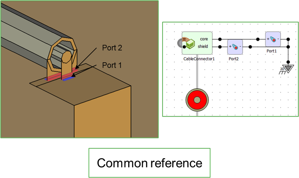
Figure 4: Combined MoM/MTL signal connection across the outer shield.

Figure 5: Signal connection relative to the shield - not over the shield.
2. Schematic link combined MoM/MTL feature
The combined MoM/MTL schematic link allows connecting cable signals to full wave geometry with full coupling between the MTL and full wave domains.
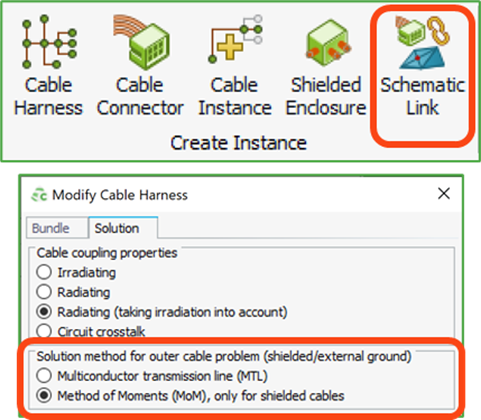
Figure 6: Schematic link component represented in the Graphical User Interface (GUI).
The schematic link allows modeling:
- The effect and radiation of non-ideal shield connections - pigtail connections, see Figure 7.
- The effect and radiation of common mode currents along the cable between devices connected at the cable terminals, see Figure 8.

Figure 7: Shielded two wire cable – shield connected via pigtail to enclosure; wires connected inside the enclosure.

Figure 8: Shielded two wire cable – wires and shield connected to PCB.
The cable signal connections to the full wave geometry can be done via a combination of: single core cables, points, geometry ports - edge port, segment port, vertex port and FEM line port. The best practice would be to use port connections as this gives more detail of the connection and what needs to be solved.
For a validation example consider a shielded two-wire cable where the two wires are connected to two traces on a simple PCB, see Figure 8 and Figure 9. The PCB is connected to a metallic box which in turn is connected to an infinite PEC plane. The shield of the cable at the other side of the cable connects with a vertical plate to the PEC plane. For a reference solution a full wave model (physical model) of the two-wire shielded cable and the PCB is solved.
Calculate 50 Ohm S-parameters between all four ports (two on the cable and two on the PCB) and near fields associated with each port active for 100 MHz to 1 GHz. The associated cable schematic is shown in Figure 10.

Figure 9: Validation example of a shielded two-wire cable connected to a grounded PCB.

Figure 10: Cable schematic setup for the connection between the cable and the full wave geometry.
Figure 11 and Figure 12 show good agreement between the full wave model solution and the combined MoM/MTL solution for the S-parameters and total H-field above the cable assembly, respectively.

Figure 11: Selected S-parameter comparison between the full model solution and combined MoM/MTL solution.

Figure 12: Total H-field 100 mm above cable assembly at 1 GHz: Port 3 active; transmit power 0.5 W.
The schematic link supports SEP, FEM and VEP dielectric models. A limitation of the schematic link solution is that impressed sources and plane waves are not supported.