Negative Power Loss of Dielectric

Hi, Everyone!
I am new to Feko and Antenna Design in general. I am trying to model a simple turnstile antenna for a 1-Unit CubeSat, which then I am going to build using tape-measure (as conductors of turnstile antenna) and a PCB in the middle for feed circuit.
here is a link where you can learn more about CubeSats (if needed):
https://www.isispace.nl/cubesats/
When I model the antenna in Feko, there's always at least one dielectric region that has negative power loss in *.out file.
For example, when I model the antenna without metallic body of CubeSat, image 1 shows the negative power loss in *.out file and image 2 shows the far field pattern.
When I add the metallic body, images 3 and 4 show the results.
I have also attached my CAD files.
Can you tell me why this negative power loss happens and how can I fix it?
And also, what other ways can I use to validate my results? Since, radiation pattern in image 4 doesn't seem correct to me /emoticons/default_smile.png' srcset='/emoticons/smile@2x.png 2x' title=':)' width='20' />
Thank you very much,
Yasaman Parhizkar
<?xml version="1.0" encoding="UTF-8"?>
<?xml version="1.0" encoding="UTF-8"?>
<?xml version="1.0" encoding="UTF-8"?>
<?xml version="1.0" encoding="UTF-8"?>
Find more posts tagged with
Thank you very much, Torben Voigt!
I used your corrected file and it didn't have any problems in power calculation!
However, I didn't trust the FEM method, since it gave me very different results compared to MoM, even when I simulated a simple wire turnstile!
So, in my next try with MoM, I moved the PCB board to provide a 1cm distance between PCB and the purple body. this time the negative loss problem was solved!
Thank you again for your kind reply!
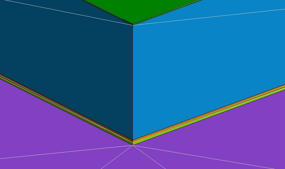
Hi @Yasaman,
the layered dielecrics are very thin comared to the wavelength:
<?xml version="1.0" encoding="UTF-8"?>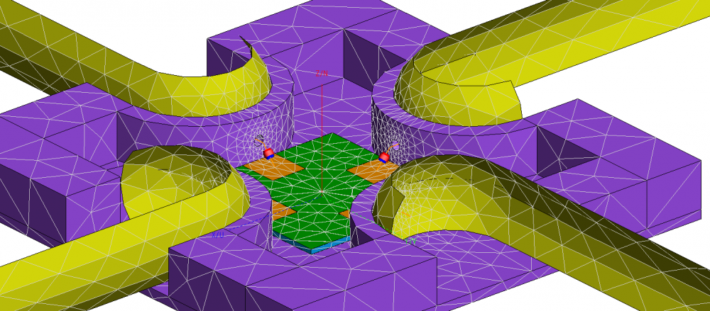
I don't think you will be successful wit MoM. It may be feasible to use FEM instead.
I attach a FEM version of the model but you will need to see if reducing the mesh size of the thin dielectric layers changes the results.
Unable to find an attachment - read this blog