Submitted by cbonnet on Tue, 03/23/2010 - 20:39
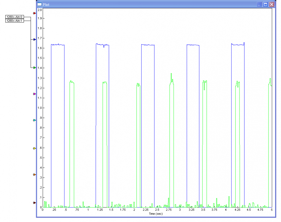
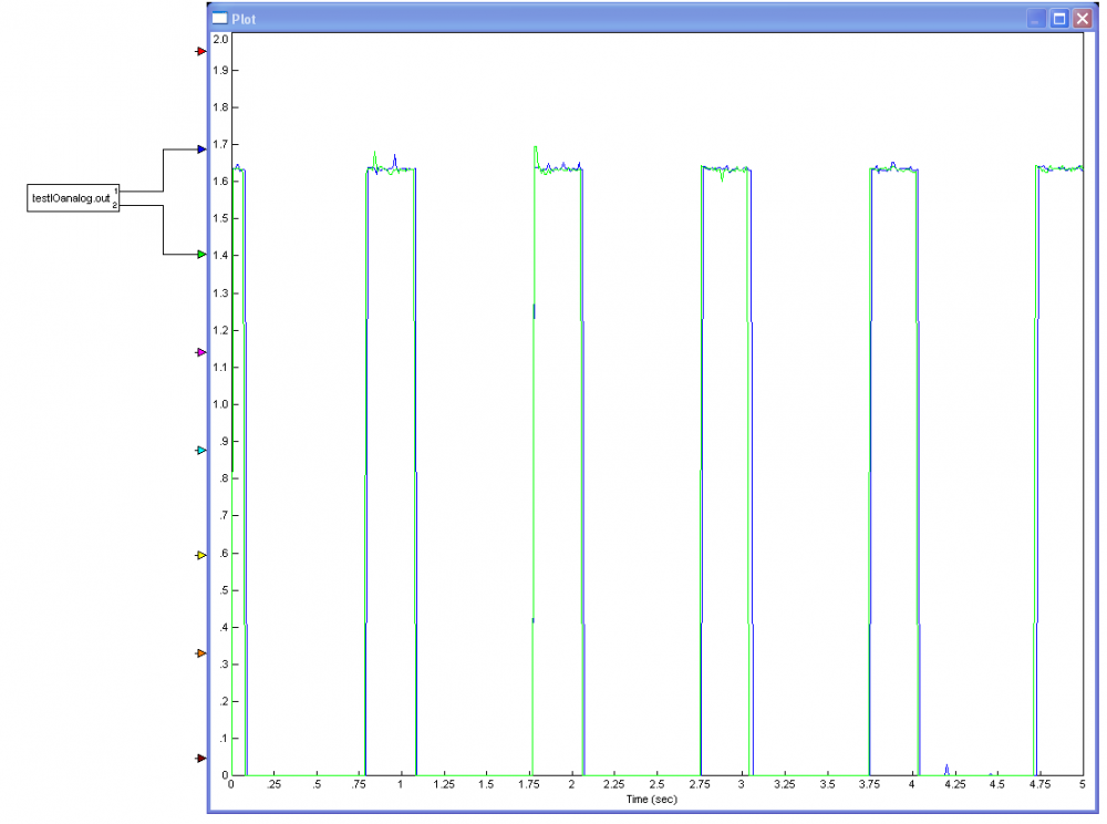
When i'm monitoring the analogic outputs of my F2808 board i get the values i'm sending from my GBF source. In the meantime, when i'm using the classic debug method consisting in putting all the diagram in a unique compound, and then compile it with the 'include vissim communication interface' option, and finally running it in another diagram using the DSP-interface : all the analogic inputs are giving the same values, whereas the 2 signals they get are different. I already read the documentation and tried modifying the settings of the ADC converter, but without success.
Please find attached to this request 2 screenshots that respectively show the hoped result, and the actual results i get with my signals.
<?xml version="1.0" encoding="UTF-8"?>
<?xml version="1.0" encoding="UTF-8"?>
Unable to find an attachment - read this blog