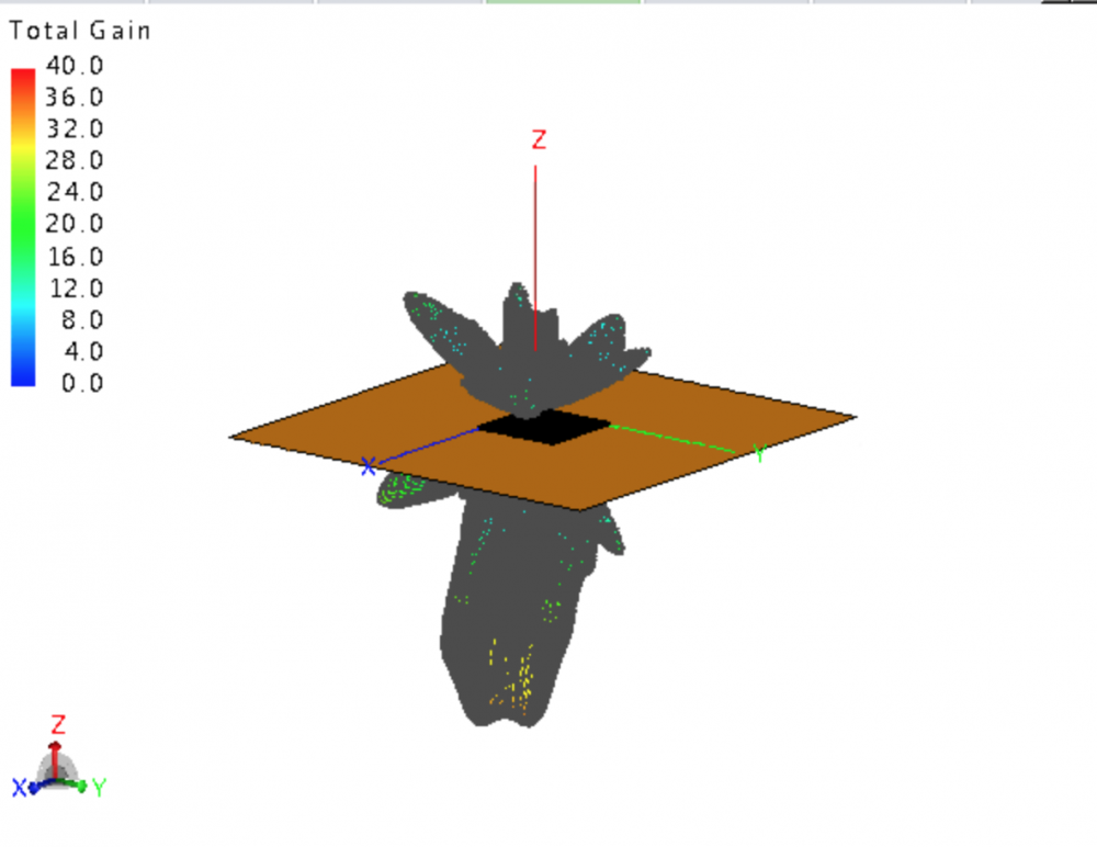
Far field pattern from an Electric near field
Hi all,
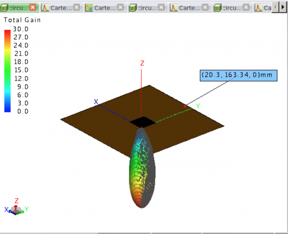
I wanted to understand how the far field from a near field response from another simulation works. I have a circular waveguide junction problem where I find the aperture field distribution and make it the input of the next simulation as a source to find the far field from it. I have put a PEC surface around the near field source (Not above or below) so that the near field acts as a slot (magnetic virtual current source). I expected to see radiation towards both half of the space but I see on one side like as if there is a PEC surface below that too. However, for some other configuration I do see some radiation towards the other half space. I wanted to understand what exactly happens.
I am attaching both models.
<?xml version="1.0" encoding="UTF-8"?>
Answers
-
Please attach the efe/hfe files, thanks.
If you can also the model that was used to generate the efe/hfe files.
0 -
0
-
It may not be related to the original problem, but in the last model you attached, why are there two apparently identical sources on the same port?
If you meant to place wgsource2 on the opposite port, where is the energy supposed to go with both ports active?
Or did you mean to make the bottom port absorbing? You don't need to place a source there then if it is only meant to absorb/sink energy. You can set the modes the port needs to absorb on the Advanced tab of the waveguide port dialog.
0 -
Altair Forum User said:
It may not be related to the original problem, but in the last model you attached, why are there two apparently identical sources on the same port?
If you meant to place wgsource2 on the opposite port, where is the energy supposed to go with both ports active?
Or did you mean to make the bottom port absorbing? You don't need to place a source there then if it is only meant to absorb/sink energy. You can set the modes the port needs to absorb on the Advanced tab of the waveguide port dialog.
Yes, I wanted to make the bottom port as absorbing. Therefore, I used the modes I wanted and set the excitation to 0 for those modes. In the advanced tab, it only asks for maximum m and n indices of the modes. Should I write the maximum values of m and n for the modes I consider? It doesn't say anything about TE or TM.
0 -
Yes, write the m and n values. Whether it is TE or TM is done automatically.
The higher m and n, the smaller the mesh size required will be.
0 -
Altair Forum User said:
Yes, write the m and n values. Whether it is TE or TM is done automatically.
The higher m and n, the smaller the mesh size required will be.
Yes, I did that. Thanks for this input.
0 -
Altair Forum User said:
Yes, write the m and n values. Whether it is TE or TM is done automatically.
The higher m and n, the smaller the mesh size required will be.
Hi @mel,
Did you, by any chance, check the original problem?
0 -
Please rerun the model capturing the near fields with the correct port settings and then verify if the original problem is still there.
If so, please attach the updated files.
0 -
Altair Forum User said:
Please rerun the model capturing the near fields with the correct port settings and then verify if the original problem is still there.
If so, please attach the updated files.
I am attaching a new simulation where the port settings are good. I have one port excited with one mode and the other port is absorbing all the energy. I am attaching the cfx file (Cone_7cm_TE11.cfx) where I generate the near fields and the cfx file where I use the near fields (FF_cone_7cm_TE11.cfx) and the near field files as well. Here, I also use a metal plane around the near field source such that the source acts like a slot. Therefore, I should see radiation to both sides of the space and I still see the radiation to one half of the space.
0