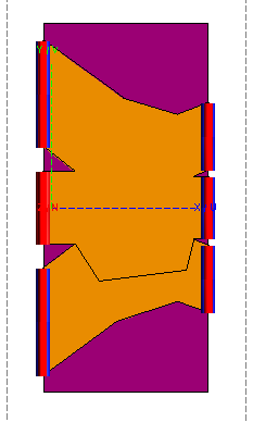
Hi, i have a very large electrical microstrip structure(lamda=5.7[mm] and dimensions of structure are 250x560[mm]) on a very thin dielectric substrate with height=0.1[mm].My structure has three ports as input and three as output.I'm using the RL-GO solver for both the microstrip region and the substrate. However when i simulate it, i'm getting the warnings: WARNING 33751: Requirements for applying the GO approximation are not met (distance to ray source too small) when the mesh is finer, and when when i make the mesh a little more coarse for les simulation time i get a warning wich says Requirements for applying the GO approximation are not met(angular pattern is too coarse). Another thing is that simulation time is pretty large and i have to run many simulations to make impedance matching networks feed lines etc..Can anyone help me to understand these warnings and how to solve them but also how could i make the simulation time less? Thank you. (Note that in the attached image the whole structure is a union but when i simplified it the edge that appears inside the structure could not be removed although there is not gap between the connected parts of the structure)
<?xml version="1.0" encoding="UTF-8"?>