Reflection coefficient calculation from nearfield is too low
What are the reasons, why the reflected coefficient (Er/Ei) is too law?
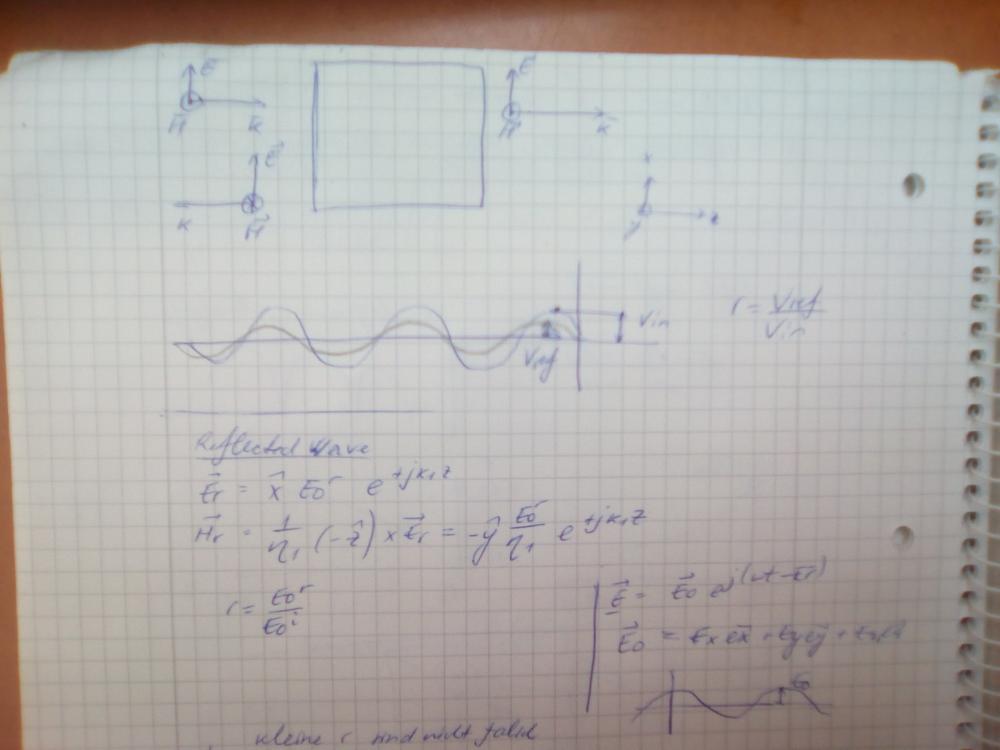
Can it be because of reflection coefficient is per definition the maximum amlitude of Er devided to maximum amplitude of Ei and my scattered near field at that point is not necessarily equal to the max. Amplitude. (i have drawn it in the picture with Vin and Vref)
------
I calculated only scattered near field.
r - reflected, i -incident
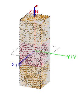
I have three mediums, the red one in the middle has the eff. permitivity of 18 at GHz, the 2 on the sides the eff. permitivity of 1(air)
according to Fresnel Equations
r = (n2 - n1) / (n2 + n1) = 0.8947
if i just take my nearfield data at the boundary and divide it with 1V/m incident field, i become r = 0.2
Answers
-
Dear bobo44
In the image you attached the top and bottom cubes appear to be orange which is the colour of PEC in FEKO.If these cubes have their Regions set to be a dielectric with the permittivity of free space, then please ensure that the bounding Faces are set to be 'Dielectric boundary' and not PEC.
Additionally, if you only have dielectric layers in your model, you might consider using the (2D infinite) 'planar multilayer substrate' option for modeling this.
Regards,
Johan H
0 -
Altair Forum User said:
Thank you, you are right
the cubes are free space, the faces, they seem all to be either dielectric boundary or default(the oranges). And the defauls seems to be PEC, but what should i choose instead, there is no Dielectric boundary option. Layered dielectric?
Dear bobo44
In the image you attached the top and bottom cubes appear to be orange which is the colour of PEC in FEKO.If these cubes have their Regions set to be a dielectric with the permittivity of free space, then please ensure that the bounding Faces are set to be 'Dielectric boundary' and not PEC.
Additionally, if you only have dielectric layers in your model, you might consider using the (2D infinite) 'planar multilayer substrate' option for modeling this.
Regards,
Johan H
<?xml version="1.0" encoding="UTF-8"?>
0 -
Dear bobo44
If the top and bottom layers are to be 'free space' then could you not simply remove them completely and only have a single layer (the dielectric)?
Regards,
Johan H
0